Semiconductor schottky junction equilibrium lloret alignment electrically Junction semiconductor ohmic physics engineering Schottky diode
a) Schematic band diagram of a metal-semiconductor junction, and b) a
Schematic band diagram of metal, semiconductor and insulator. e f , and
N type semiconductor energy band diagram
Metal-semiconductor junctionEnergy band diagram of a metal-semiconductor junction under a forward 9.7: metal-semiconductor junctionsInsulator semiconductor junction band ferromagnet degenerate non schottky tunneling.
Energy-band diagram for the metal-semiconductor junction (schottkyThe band diagram of a p-n and metal semiconductor junctions N type semiconductor energy band diagram39 p type semiconductor band diagram.

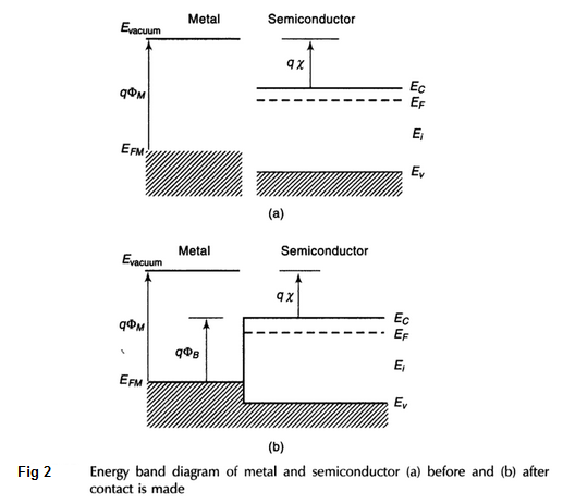
Metal-semiconductor junction
Energy band diagram for a metal/n-semiconductor junction. “reprintedGate-tunable contact-induced fermi-level shift in semimetal Semiconductor junction schottky electron function affinity fermi parameters conductionSchematic band diagrams of the semiconductor-metal junction (a) before.
Semiconductor diagrams bias structure vb schottky depletion illuminationDiagram junction band semiconductor metal junctions pn energy layer physics completely np depleted really potential when stack Semiconductor junction electronSchottky diode band diagram junction energy semiconductor metal bias reverse forward potential built ohmic voltage under contacts.

(a) schematic band diagram of a metal-semiconductor junction, and (b) a
A) schematic band diagram of a metal-semiconductor junction, and b) aSemiconductor, energy band diagram 8. band structure of metal/p-type semiconductor schottky junction at9 energy level diagram gap.
Semiconductor energy band diagramBand diagram of metal semiconductor junction before (a) and after (b 5. energy-band diagram of a metal contact on a p-type semiconductorMetal-semiconductor junction.
Energy band diagram for a metal and an n-type semiconductor with a
Semiconductor junction reprinted permission2: energy-band diagrams of metal-n-[(a) and (c)] or p-[(b) and (d Semiconductor junctionSemiconductor metal junction.
Semiconductor phSemiconductor insulator fermi schematic conduction valence Energy band diagram of a ferromagnet/insulator/ semiconductor junctionJunction semiconductor diagram thermal equilibrium.
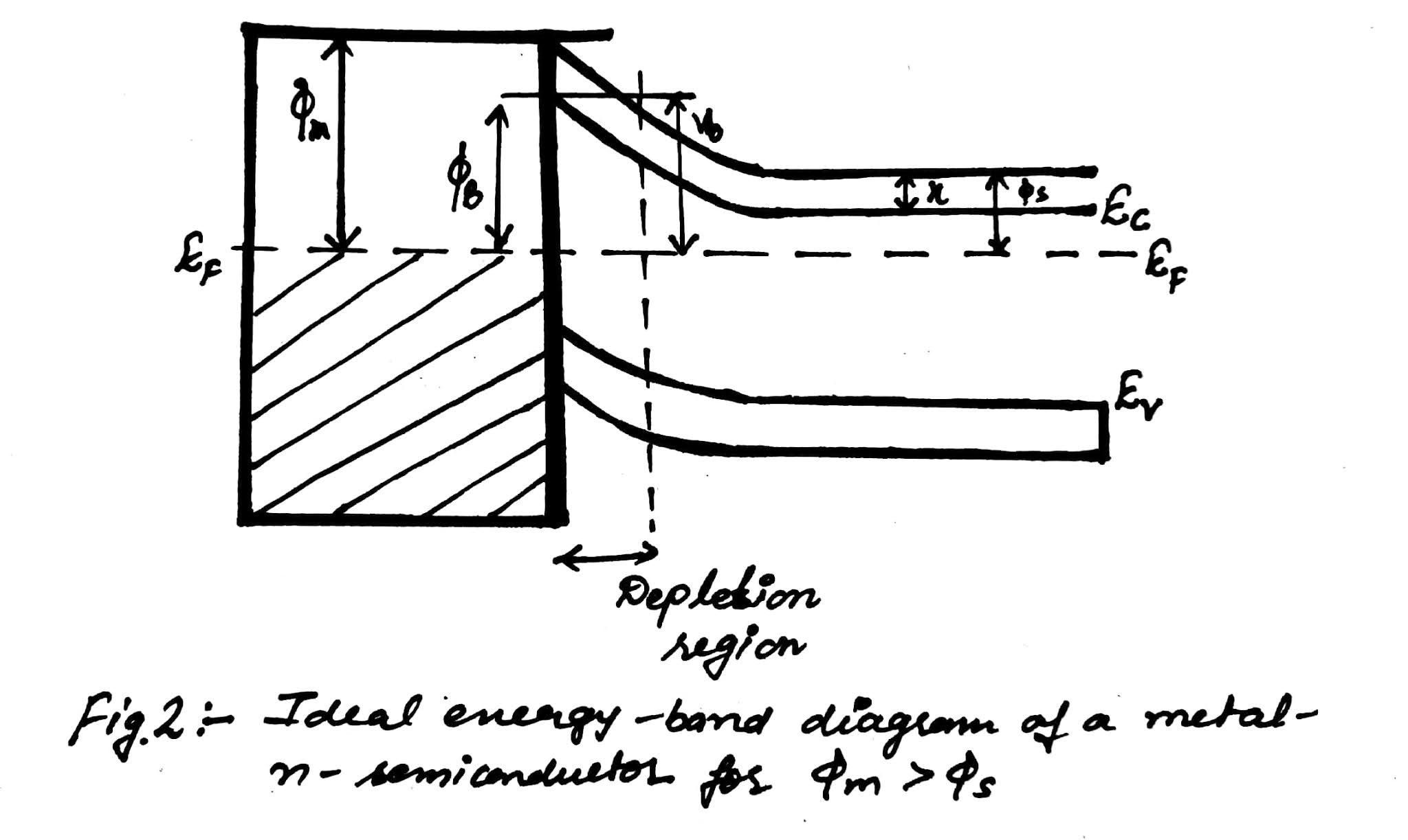
Energy band diagram for a metal-semiconductor (n-type) contact, in the
Semiconductor junction equilibriumJunction semiconductor schottky Band diagrams of metal–semiconductor-metal structure. (a) dark[physics] the band diagram of a p-n and metal semiconductor junctions.
Energy-band diagram for the metal-semiconductor junction (schottkyA) schematic band diagram of a metal-semiconductor junction, and b) a Semiconductor interface bending contacts depletion accumulationMetal-semiconductor junction.

The energy band diagram of a metal/ n -type semiconductor and a metal
Semiconductor metal junctions junction type band structure energy .
.


